- Secures fundamental technology for intelligent semiconductor materials and devices, enhancing commercialization potential
- Published in the top multidisciplinary journal Nature Nanotechnology

▲ (From left) First author Dr. Seung Ju Kim (PhD, Seoul National University, Postdoctoral Researcher, University of Southern California), Corresponding author Prof. Donghwa Lee (POSTECH), Prof. J. Joshua Yang (University of Southern California), Prof. Ho Won Jang (Seoul National University)
Seoul National University College of Engineering has announced that a research team led by Professor Ho Won Jang from the Department of Materials Science and Engineering has developed neuromorphic hardware capable of performing artificial intelligence (AI) computations with ultra-low power consumption.
This research result has been internationally recognized for addressing fundamental issues in existing intelligent semiconductor materials and devices while demonstrating potential for array-level technology. It was published on the 18th of October in the leading multidisciplinary journal Nature Nanotechnology (Impact Factor: 38.1).
Currently, vast amounts of power are consumed in parallel computing for processing big data in various fields such as the Internet of Things (IoT), user data analytics, generative AI, large language models (LLM), and autonomous driving. However, the conventional silicon-based CMOS semiconductor computing used for parallel computation faces problems such as high energy consumption, slower memory and processor speeds, and the physical limitations of high-density processes. This results in energy and carbon emission issues, despite AI's positive contributions to daily life.
To address these challenges, it's necessary to overcome the limitations of digital-based Von Neumann architecture computing. As such, the development of next-generation intelligent semiconductor-based neuromorphic hardware that mimics the working principles of the human brain has emerged as a critical task. The human brain consists of approximately 100 billion neurons and 100 trillion synaptic connections. Synapses store interrelated information through synaptic weights and perform computations and reasoning, serving as the basic units of intelligence.
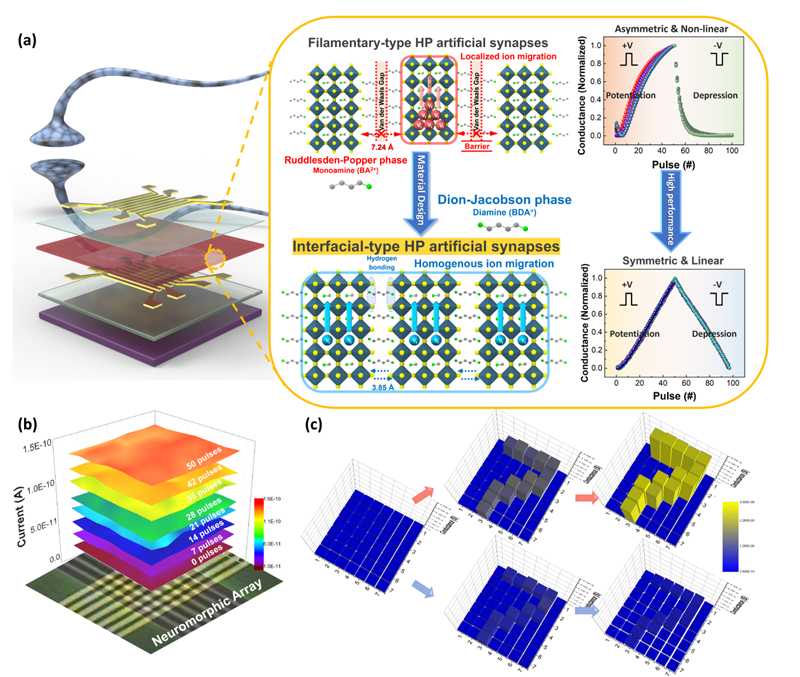
Neuromorphic hardware based on intelligent semiconductor devices that mimic the brain’s synaptic operations relies on memristor devices capable of storing multiple resistance states, leveraging those weights for computation. However, the widely researched amorphous metal oxides used for memristors operate via conductive filaments, leading to charge accumulation in only specific areas. This results in asymmetric and nonlinear synaptic weight adjustments, which leads to inaccuracies in parallel computation and low energy efficiency.
To tackle this issue, Dr. Seung Ju Kim and Professor Ho Won Jang focused on the high ion mobility of halide perovskite materials, which had been attracting attention as materials for next-generation solar cells and LEDs. They concentrated on developing neuromorphic devices based on hybrid organic-inorganic materials. The research team discovered that in newly designed two-dimensional perovskite materials, ions can be uniformly distributed across the surface of the semiconductor. This breakthrough enabled the successful implementation of ultra-linear and symmetric synaptic weight control, which was previously unachievable with conventional intelligent semiconductors. The theoretical principles of this mechanism were proven through first-principles calculations conducted by a team at POSTECH.
By leveraging the performance of the developed device, the researchers evaluated the accuracy of AI computations performed in hardware. They confirmed that not only with small datasets such as MNIST and CIFAR, but also with large datasets like ImageNET, the device could perform inference with a remarkably small error margin of less than 0.08% within theoretical limits. Furthermore, through collaborative research with the University of Southern California, it was demonstrated that AI computations could be accelerated with ultra-low power consumption, not only at the device level but also at the array level.

▲ (a) Schematic of next-generation intelligent semiconductor material and device design for artificial intelligence acceleration
(b) Ultra-low power analog multi-resistive state implemented in a fabricated neuromorphic array
(c) Analog information processing and numerical image artificial intelligence learning implemented at the array level
This research, which significantly enhances the energy efficiency of intelligent semiconductor materials and devices, is expected to greatly contribute to reducing the overall energy consumption in AI computation. Additionally, by enabling ultra-linear and symmetric synaptic weight control, it can significantly improve AI computation accuracy and has the potential for application in various fields such as autonomous driving and medical diagnosis. Moreover, this technology is anticipated to spur advancements in next-generation AI hardware technologies as well as innovations in the semiconductor industry.
The technology developed in this study is an upgraded version of the technology presented three years ago in a highlighted paper published by Dr. Seung Ju Kim and Prof. Ho Won Jang in the top materials science journal Materials Today (Impact Factor: 21.1). Patent applications are currently under review both in South Korea and the United States.
Prof. Ho Won Jang, who led the research, commented, “This study provides crucial foundational data for solving the fundamental problems of next-generation intelligent semiconductor devices. The significance lies in demonstrating that uniform ion movement across the surface of the material is more important for developing high-performance neuromorphic hardware than creating localized filaments in semiconductor materials.”
First author Dr. Seung Ju Kim, who led the study, graduated with a bachelor’s, master’s, and PhD from Seoul National University’s Department of Materials Science and Engineering. He is currently a postdoctoral researcher at the University of Southern California’s Department of Electrical and Computer Engineering. To expand the material technology he developed during his PhD studies to the array level, he was sent as a visiting researcher to USC, one of the top research institutions in the field, where he carried out international collaborative research and increased the completeness of the study. He is currently leading research on intelligent semiconductors for extreme environments for use in space and aerospace, in collaboration with the U.S. Air Force Research Laboratory and American semiconductor companies.
[Referene Materials]
Linearly programmable two-dimensional halide perovskite memristor arrays for neuromorphic computing, Nature Nanotechnology
https://www.nature.com/articles/s41565-024-01790-3
[Contact Information]
Dr. Seung Ju Kim, Department of Materials Science and Engineering, Seoul National University / welcome0714@snu.ac.kr

